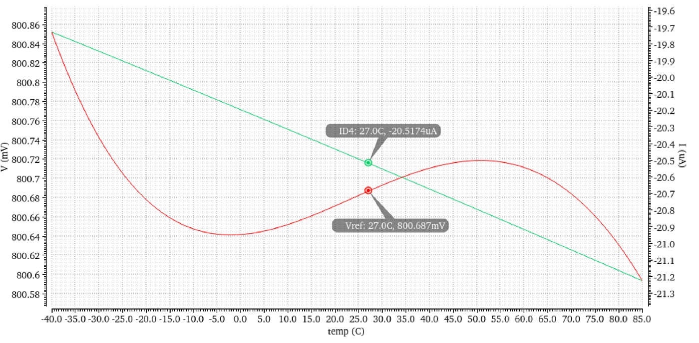
Four lab exercises for the Analog Integrated Circuit Design course at the University of Padova (Prof. Andrea Neviani), each following the same discipline: hand-calculate the circuit first, then simulate it in Cadence Virtuoso, and reconcile the two when they disagree. In order: characterizing CMOS current mirrors, sizing a fully-differential OTA to a gain/bandwidth/offset spec, compensating that OTA inside a capacitive-feedback loop so it stops ringing, and tuning a band-gap reference until it stops drifting with temperature. All four are summarized below, with the full calculations, plots, and corner/Monte-Carlo analysis in the linked report.
Lab 01
Where a current mirror stops mirroring
The mirroring ratio IOUT = N·IIN only holds exactly at one operating point — everywhere else, channel-length modulation, DIBL, and narrow-width effects pull the two branches apart. Corner simulations (TYP/SS/FF) and a 100-run Monte Carlo sweep quantified how much: a predicted 7.95 μA mismatch spread against a simulated 5.01 μA, close enough to trust the hand model. Redesigning the mirror as a wide-swing cascode then pushed the output resistance from 1.8 MΩ to well past spec while keeping the current error under 1%.
Lab 02
Sizing an OTA to a hard spec
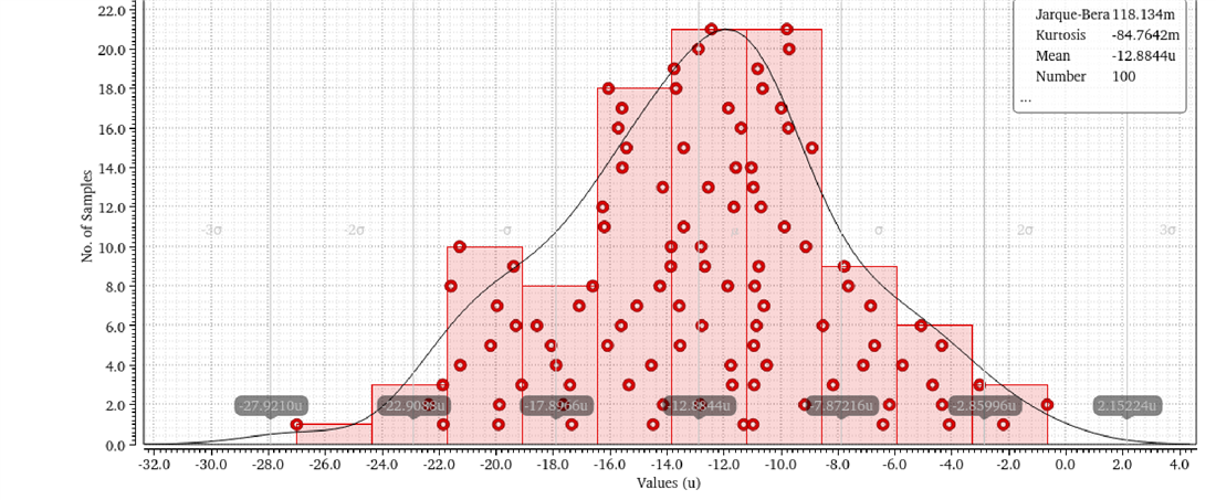
The initial sizing of a fully-differential, current-mirror-loaded two-stage OTA fell well short of target: 14.2 dB of gain and 54 MHz of bandwidth against a 30 dB / 1 GHz requirement. Since gain and bandwidth are set by nearly independent quantities — the mirror ratio and tail current fix the bandwidth, the output-device length fixes the gain at that bandwidth — raising the mirror ratio to 7.5, the tail multiplier to 6, and lengthening the output devices closed both gaps at once, and widening the input pair pulled the offset back under spec too.
Lab 03
From 25° of phase margin to a clean 20 ns settle
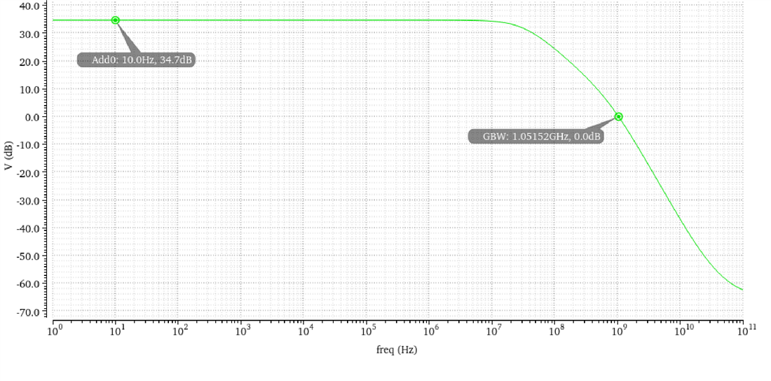
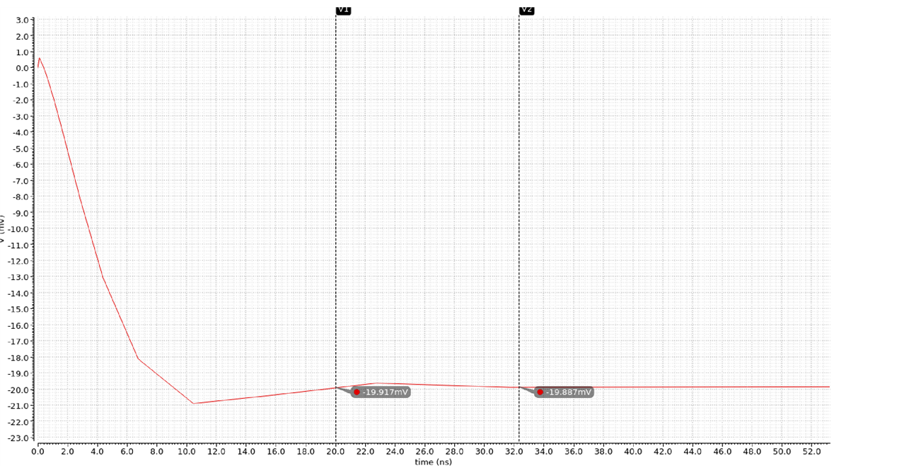
Close a two-stage OTA inside a capacitive-feedback loop and its two internal high-impedance nodes — two poles sitting close together, plus a right-half-plane zero baked into the topology — leave it barely stable: 25° of phase margin and a step response that rings for microseconds. Splitting the poles with a Miller capacitor and a nulling resistor, then redesigning the bias currents and device sizing around the target specs, turns that into a clean settle in about 20 ns with 68.5° of margin.
Uncompensated
Compensated
Try it — drag to add Miller compensation
Illustrative reconstruction from the reported phase-margin and settling figures above, not the original simulation waveform.
Lab 04
Tuning a band-gap reference flat to 0.09%
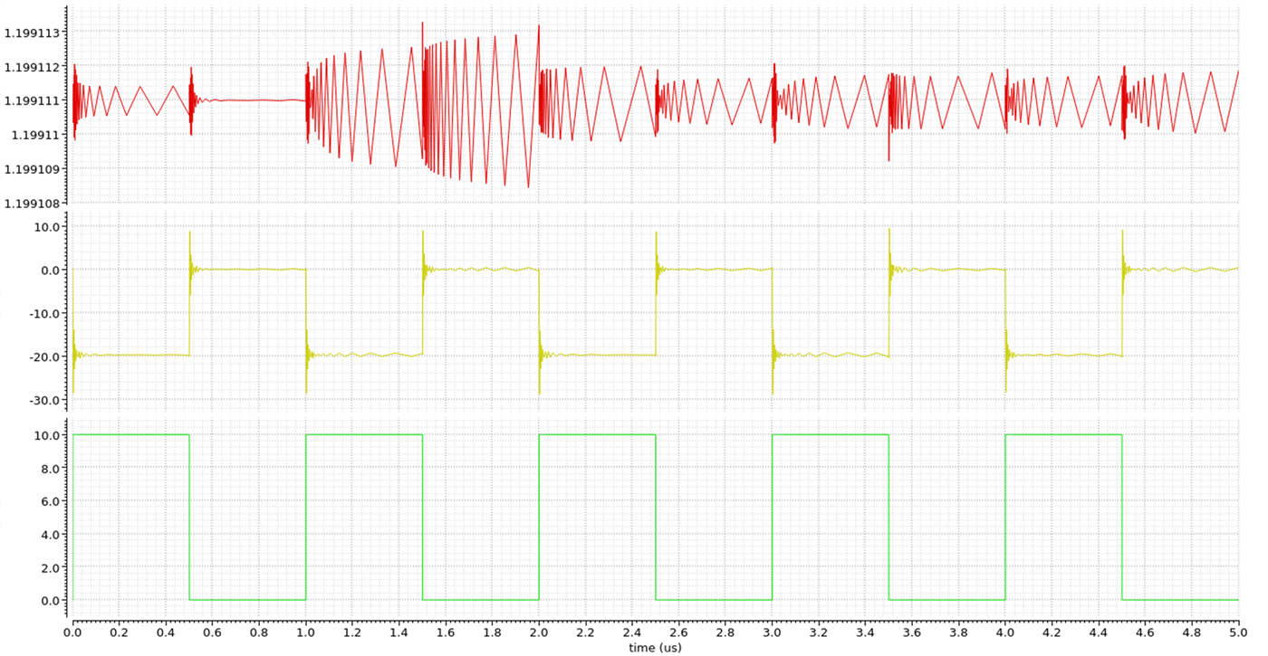
A low-voltage band-gap reference sums a CTAT diode voltage with a PTAT resistor voltage so the two temperature dependencies cancel out. The first hand-calculated sizing landed 7.6% high on the reference voltage with a visible slope over temperature — traced back to a small offset in the feedback amplifier that balances the two branches, which skewed the mirror current. Retuning the three resistors one at a time (fix the bias current, null the slope, recentre the output) brought the reference within 0.086% of the 0.8 V target, essentially flat from −40 °C to 85 °C.